Friday, August 26, 2022

Vector Network Analyzer ( VNA) - 2 - Screenshots

During writing of by blog post, that originally was planned as the second post in this VNA series,  i realized that i wanted to show very much pictures in one blog post.
Therefore first this post "Vector Network Analyzer ( VNA) - 2 - Screenshots" with some screenshots of some parts of the VNA software and settings that i used before i will present Vector Network Analyzer ( VNA) - 3 - RF Demo Kit measurements.

The LiteVNA 


Settings I used when testing the RF Demo Kit

Window for Calibration


Frequency ranges (can be stored in the Windows software)


RF Demo Kit

Vector Network Analyzer ( VNA) - 1 - Intro

Recently i received my Vector Network Analyzer (LiteVNA) and am very happy to finally have this interesting device.


Information and explaining in detail what is a VNA, what you can do with it (and how) can be found on internet and is probably better explained by other who have much more experience with this topic. However as i want to post some first results when testing my VNA on my blog, and for visitors of my blog who don't know anything about VNAs i first need do start with "Vector Network Analyzer ( VNA) - 1 - Intro". 

A Vector Network Analyzer (or VNA) is an electronic measurement and testing device that generates and measures frequencies so you can do measurements on things like antennas and (radio) frequency filters.
With modern electronic and some smart people made it possible to buy now a VNA in the 50 Euro range to do some measurement that where some years ago only possible with equipment of thousands of euros. The LiteVNA that i got costs around 100 Euro as this device works up to 6 GHz. My first 3 attempts some months ago to buy a VNA failed. After ordering i received a message it was not possible to deliver and my money was returned. I even did think of buying a VNA with lower frequency range if it was available. However, after some weeks waiting, i tried again at another store and they could deliver relative fast! The VNA came with a Short Open and Load connectors and some cables.

The VNA has two connectors. One connector acts as a combined output and input. A signal is provided to a DUT (Device Under Test)  and the signal is measured. The frequency of the signal can sweep in a frequency range and this way you can determine frequency characteristics of an antenna.
The other connector can act as input and by placing a DUT (a filter circuit) between the output and input you can observe how the DUT (filter circuit) behaves at different frequencies.

Calibration of the VNA is very important and the VNA also reacts on other changes e.g. cable length. A common calibration is the SOLT calibration  (Short, Open, Load and Thru).
Short Open and Load calibration is done by using a shorted circuit, open circuit or a load (e.g. 50 Ohm) on the combined input/output and running the appropriate calibration.
Calibration of Thru is done by connecting the two connectors without the DUT running the Thru calibration.

The LiteVNA can be used stand alone (powered provided by build in Lithium power cell) or via USB connected to a computer. Usng the computer you have a much bigger screen and you can easy export the measured data or  the pictures. The LiteVNA also as a memory slot for additional storage.
As recommended by some internet tutorial I placed additional connectors on the original connectors for protection.

In my next blog post i will post some results using a RF Demo Kit board. 

Some findings in the limited time that i have played with the VNA:

  • It is nice that the PC software can display a graph of the battery power of the VNA.
  • The LiteVNA (at least mine) can become very warm. Perhaps some settings (output power) can or need to be adapted to reduce this. I could not yet find if the temperature can be monitored (like the battery power). I don't know if and and how measurements are influenced by this temperate.
  • Measurements seems to be quite sensitive to things like cable length and the connection.

Tuesday, June 28, 2022

Non sequential computing environment and Forth -1-

Some things described in this article series can be used to implement the Forth programming language in a 'non sequential computing environment' and in a 'sequential computer environment..

My first reason to write this article series with the name 'Non sequential computing environment and Forth' is that non sequential computing can bring much computer power and will be easy to scale up if it is simple to use. It is called  'non sequential computing environment' as the terms parallel computing, parallel processing , concurrent computing or multitasking as give associations to to specific other things and solutions. ( https://en.wikipedia.org/wiki/Parallel_computing can help to give some background ) 

A second reason that this article series can be an inspiration for new Forth implementations and has items that can be used in a real implementation by others.

I am experimenting with new Forth implementations and want to report something about it. The third reason for writing this article series is that it can serve as an introduction to my experiments.

I the early days of computers was the cost of the hardware was an important limiting factor

You needed to spend a months salary for a 'simple' computer like a Commodore 64. To get more computing power the most easy way seemed to be is doing everything at a higher speed. Every evolution creating a next generation faster computers (and making the old computers obsolete).

A new fast computer is still relative expensive however there are also a lot of cheap computing devices available. Special hardware ( e.g. FPGA's , small micro controllers, memory ) is getting more and more available for low prices. Yes the newest and fastest hardware is still expensive however the price of getting computer power is extreme low compared to 40 years ago.

Small cheap processors and micro-controllers and FPGAs do have this interesting computing power. For only a few euro's or dollars it is possible to buy devices like raspberry (or other) pi systems or devices like ESP8266 or ESP32. When you look to the hours you need to work to earn sufficient to buy, several years ago, one computing device', nowadays can can buy more than hundred ESP32 devices. The only problem is that we do not (yet) have good software tools to handle that amount of computing power.  

In the 'classic' computer evolution the computer power was increased by a higher clock speed, adding memory caches special instructions and some other tricks. Processes and programs are executed sequential and the speed is increased to get more computing power. If we sacrifice some of the computer speed and could do things non sequential it is possible to scale up extremely by doing things in parallel. Perhaps this even creates 'greener' computers as old computer power does not become obsolete but can still be used as everything is non-sequential.

My opinion is that especially the programming language Forth can play a roll in a non sequential computing environment. Many programmers are trained in sequential programming and thinking. Also most programming languages are created in a sequential way.  Therefore also a mind shift is needed.
I will illustrate non sequential programming with some simple standard examples. Let say we have a simple problem with 2 variables. 

In a non Forth environment e.g.:
A = 5
B = 3
We want to swap the values so A will have the value of B and B will have the value of A.
In most languages it is not possible to put this in a program like
Let A = B
Let B = A
This as everything is executed sequential. In our example first A will get the value 3 ( the value of B ).
And in the second statement B will get the value of A. However at that moment A has the value of B (= 3 ) so in the end A as well as B both will have the value  3 .
In our sequential programming environment for swapping the values of A and B we need to introduce a third variable C and make a program like
Let C = A
Let A = B
Let B = C

In Forth it is a good practice to not use unneeded variables and do all calculations on the stack.
In Forth the values are manipulated on the stack.
Typing 5 3 will push the two values 5 and 3 on the stack.
With .S we can look on the stack and this can display something like (2) 5 3 showing that there a two items on the stack
When we want to swap the order in Forth we give the command SWAP
Checking again with .S gives 3 5

Can Forth do real magic and just SWAP these values in one step?
Unfortunately (most times) no!
This as SWAP (like many other Forth words) in most of the Forth implementations is build using multiple Forth high or low level commands that are executed sequential to do the 'swap'.
Sometimes a the second stack in Forth ( the return stack ) is used to temporary store the value.

A second example is the Forth word DROP . This word removes the top item from the stack. Depending how the stack is implemented in memory it also increments or decrements the Top Of Stack pointer ( the Forth variable TOS ). ( Incrementing or decrementing by 1 is a simple explanation. In fact it also depends on the hardware ( 8 or 16 bits) and the amount of bits of each item on the stack. If the stack items are 16 bits and the memory is just 8 bits the stack needs to be incremented or decremented by 2 and not by 1 ) 

A third, a little more complicated, example of Forth code. An addition.
For example
3 1 +
The values 3 and 1 are pushed on the stack. + does the addition so on top of the stack is now 4
In fact + does multiple things: Not only the two values are added. Also the top of the stack changed  (incremented or decremented depending how it is implemented in Forth.)

What if we could have a Forth that could do this in a non sequential way?
As a first step describing (and implementing) Forth commands in a non sequential way could help.
For most Forth words there are already descriptions in a more or less non sequential way. Often you see explanation of words described  like:

SWAP ( n1 n2 — n2 n1 )

n1 and n2 are the first and second item on the stack
We can represented most all (primitive) Forth words in using a (lookup ) table containing this information. See below a very simple lookup table (with the headers in bold).

Table 1.
  TOS n1  n2 n3 
 SWAP  TOS n2 n1 n3
 DROP TOS - 1
 n2  n3
  + TOS - 1
 = n1 + n2 n3

n3 illustrates that n3 did not change with any of the words SWAP DROP + 
TOS the top of (parameter) stack was also added illustrate that it changes.
E.g. DROP or + will increment TOS.
In part 2 of this article series i will write more in detail about this table.

Monday, June 20, 2022

Youtube Scam Alert

 As a response to my comment on a Youtube Video of AdamSavagesTested i found the message below:

The red T in the circle makes it look like a response from the  AdamSavagesTested account, however if fact it is from another YouTube channel created just a few weeks ago:
Below a screenshot of the conversation on Telegram:

So it turned out by pre-paying $125 for shipment i receive the prize, a MacBook of more than $1000 !
(Several other people also got a similar message that they won a prize.)

It even turned out a little more interesting. I suggested Bitcoin as payment.
Would FedEx accepting Bitcoin ??
Does the scammer really think i believe him and smells the money?


Thursday, June 16, 2022

Apps Privacy

As i am experimenting also with Android apps i also need to include a link to a privacy policy.
Some apps don't collect data and this page contains the privacy policy for this apps.

So in the itself app no data i collected, only data that is collected by Google and the app-store itself.
 

Monday, April 18, 2022

Big Clive Supercomputer Version 2022

Recently i created a new ( 2022 ) version of a Big Clive Computer. More than a year ago (January 2021) i posted on my blog my 2021 version of Big Clive's Supercomputer https://blog.jeronimus.net/2021/01/big-clive-supercomputer.html From last years version no video was posted on my blog. This year i decided to include a video.

The 2022 version is a 2 color version,  i used 2 resistors. Also in last years version to reduce the amount of components i use only one resistor per color/group of led.

The value of the resistor depends on the voltage of the power supply. ( I decided to power it with a 9 volt battery )
Components list:

  •  2*6 leds flashing leds ( 12 leds, 6 leds of each color) 
  • 2 resistors
  • 1 small switch
  • one 9 volt battery with connector
  • 1 piece of perfboard


Sunday, January 2, 2022

D2-D9 Led tester Shield for Arduino Uno

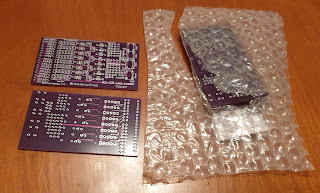
There are several shield available for the Arduino Uno that can help with learning, experimenting and testing. I created a simple "D2-D9 Led tester shield" that can be used to test some simple Arduino output. 


It is a simple PCB with 8 Leds and resistors 3 standard push buttons and a reset button.
I called my shield the D2-D9 Led tester shield. On the PCB there are no hard paths from D2-D9 to the Leds or the buttons (Except the Reset button). With some jumpers the Leds can be easy connected, disconnected or reconfigured.
Each led has a 5 pin male DuPont connector and two jumpers connected according to the diagram below.


On the first PCB i soldered i used two different color jumpers to easy show the connection. However it is also possible to do things different, e.g. using wire bridges to hard wire the Leds.
The middle pin Dn is D2 to D9. In the table below i used a (anode) and k (kathode) for the led connections. However in reality it is an Led with resistor.


 GND  k  Dn  a  VCC 
(no jumpers / nothing connected)
 led off
(See photo U2)
GNDkDnaVCC
"power mode"
 Led always on
(See photo U3)
GNDkDnaVCC
Led between GND and Dn
Dn High will turn led on
(See photo U4)
GNDkDnaVCCLed between Dn and VCC
Dn Low will turn led on
(See photo U5)
(U5 also has noting connected like U2,The jumpers are attached to one pin.) 

To connect another data-pin from the Arduino  than the corresponding Dn in the 5 in connector a Dupont wire can be used.
 I made my the PCB design versatile; for the resistors and/or Leds  SMD or Thru Hole components can be used.
On the shield is also a Reset button and 3 push buttons ( SW0, SW1 and SW2) that easy can be connected with jumpers to A0, A1 and A2.
Using my "Ardaptor design" , a design that i try to use is possible (e.g. on my PCB business card ) additional flexibility is added. I named it "Ardaptor design", a combination of Arduino and adapter, as a work name for this experiment when i first tried it. I am staring to using this name more in public. It has the following features:
-1- Next to the standard pins for the Arduino there is an additional set of holes on the PCB. In stead of Dupont connectors with extra long pins it is also possible to use just male pins and an additional set of female pins to make the shield stackable.
-2- An additional row of pins using the normal pin grid so the PCB can also be used to stack a standard veroboard  (PY-5cm*7cm) to an Arduino.
Besides the easy stacking it has the advantage that, as with the cheap PCB services you get minimal 5 PCBs, unused PCBs can be easy made useful. 

( Update 18NOV2022: Added this project to my Github https://github.com/JanJeronimus/Arduino_LedShield )

Friday, December 31, 2021

2 x Xmas ( Buzzer & Speaker )

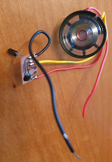
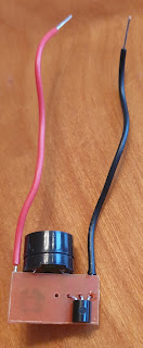
 As i have some of this cheap audio modules i wanted to heard the difference between using a buzzer and a (cheap mini) speaker. I used two similar audio modules soldered a buzzer to one and a small speaker to the other. I recorded a video to let you hear the sound using the same battery and settings on my phone.  You can hear the difference, however a buzzer is much more cheaper and as the 'music' from the module are just beeps it is much cheaper to to use the buzzer. For powering the module i used a my ÇR2032 Lithium Cell Battery "power station'.
I did screw up a part of the video as i later applied a video effect to a part of the video that also changed the audio. However there is sufficient 'untouched' audio to hear it.
If you do no want to watch the full 2.50 video here is what you can expect: 0:00 Intro 0:18 Buzzer 1:13 Speaker


The audio module is a PX088A module using a potted music chip.  "DIY Sound Module For Toy Christmas Song Music Voice Module Sound Chip Loop Play For DIY/Toy Jingle Bells 3-4.5V" and can e.g. be found on Aliexpress.
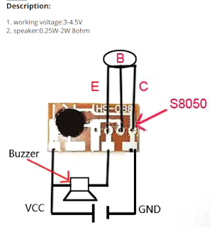
This module is also available with some other sounds. (Alice Music, Ding Dong, Bird chirp ) Unfortunately, if you have several different modules, the sound is not marked on the outside and you need to test it. Strangely there is a similar looking module marked LX9300H with a happy birthday song. An A8050 transistor (or equivalent) , a buzzer or speaker and a power source is needed to get it working using the diagram below.
It was a bit confusing that module on the circuit diagram a different number on it than the sold module: HS-088.  


Also you can find different schematics for this module ( e.g. https://leap.tardate.com/audio/audioeffectschips/px088a/ ) that i did not tried yet.
Module with mini speaker

Module with buzzer (back)
Module with buzzer (front)


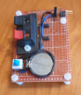
The ÇR2032 Lithium Cell Battery "power station' that i build some time ago is just a  CR2032 battery holder, a switch and some connectors on a small veroboard. It also has some plastic stands to put it on your desk. It has helped me a lot when building and testing small projects like this.
"CR2032 power station" 

Some links