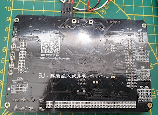
On AliExpress i also ordered the EU-STM8S207|103-DEMO board.
This board has two STM8 controllers and several hardware items.
According to info the two STM8 controlers should be able to communicate with each other.
There is a MicroSD card holder, a W2064 Flash ram, A buzzer (Beep), LDR, One reset button. Two buttons connected to the 207 and one button connected to the 103 (on which pin??), Several connectors (e.g. for ESP01 wifi),GSM. SPI, I2C AD/DA, GDM, 207-UART1 a 207-SWIM and 103-SWIM and some other items. Also additional boards to add more hardware can be ordered.
Unfortunately i could not yet find good documentation or a schematic diagram.
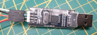
After playing with a cheap STM8S103F3P6 board i decided to try out this board and connected my ST-link (shown in an earlier post) to the 103-SWIM connector. On this board the SWIM connector indicates 5V so i used 5V. ( The STM8S103F3P6 board indicates 3V3 so there i used 3V3).
I modified the STM8S Blink sketch to the sketch below to test the output pins.
// CODE
const int LED_TT = 12;
/
pinMode(LED_TT, OUTPUT);
}
// the loop function runs over and over again forever
void loop() {
digitalWrite(LED_TT, HIGH); // turn the LED on (HIGH is the voltage level)
delay(1000); // wait for a second
digitalWrite(LED_TT, LOW); // turn the LED off by making the voltage LOW
delay(1000); // wait for a second
}
// END CODE
LED_TT is Led To Test
By changing the LED_TT value in the program above i could test the "Clock like arranged Leds".
Results are in the table below.
Clockwise 1-12
LEDs on PCB | Pin in
Script | |
| 1 | 0 | |
| 2 | 1 | |
| 3 | 2 | |
| 4 | 4 | |
| 5 | 3 | |
| 6 | 5 | |
| 7 | 6 | |
| 8 | 7 | |
| 8 | 8 | |
| 10 | 9 | |
| 11 | 11 | |
| 12 | 12 | |
Strange that the 4 and 3 are swapped. I expect Pin 10 (D10) is not used as this corresponds to SWIM in some pictures i found.


