Showing posts with label Ardaptor. Show all posts

Sunday, January 2, 2022

D2-D9 Led tester Shield for Arduino Uno

There are several shield available for the Arduino Uno that can help with learning, experimenting and testing. I created a simple "D2-D9 Led tester shield" that can be used to test some simple Arduino output. 


It is a simple PCB with 8 Leds and resistors 3 standard push buttons and a reset button.
I called my shield the D2-D9 Led tester shield. On the PCB there are no hard paths from D2-D9 to the Leds or the buttons (Except the Reset button). With some jumpers the Leds can be easy connected, disconnected or reconfigured.
Each led has a 5 pin male DuPont connector and two jumpers connected according to the diagram below.


On the first PCB i soldered i used two different color jumpers to easy show the connection. However it is also possible to do things different, e.g. using wire bridges to hard wire the Leds.
The middle pin Dn is D2 to D9. In the table below i used a (anode) and k (kathode) for the led connections. However in reality it is an Led with resistor.


 GND  k  Dn  a  VCC 
(no jumpers / nothing connected)
 led off
(See photo U2)
GNDkDnaVCC
"power mode"
 Led always on
(See photo U3)
GNDkDnaVCC
Led between GND and Dn
Dn High will turn led on
(See photo U4)
GNDkDnaVCCLed between Dn and VCC
Dn Low will turn led on
(See photo U5)
(U5 also has noting connected like U2,The jumpers are attached to one pin.) 

To connect another data-pin from the Arduino  than the corresponding Dn in the 5 in connector a Dupont wire can be used.
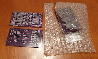
 I made my the PCB design versatile; for the resistors and/or Leds  SMD or Thru Hole components can be used.
On the shield is also a Reset button and 3 push buttons ( SW0, SW1 and SW2) that easy can be connected with jumpers to A0, A1 and A2.
Using my "Ardaptor design" , a design that i try to use is possible (e.g. on my PCB business card ) additional flexibility is added. I named it "Ardaptor design", a combination of Arduino and adapter, as a work name for this experiment when i first tried it. I am staring to using this name more in public. It has the following features:
-1- Next to the standard pins for the Arduino there is an additional set of holes on the PCB. In stead of Dupont connectors with extra long pins it is also possible to use just male pins and an additional set of female pins to make the shield stackable.
-2- An additional row of pins using the normal pin grid so the PCB can also be used to stack a standard veroboard  (PY-5cm*7cm) to an Arduino.
Besides the easy stacking it has the advantage that, as with the cheap PCB services you get minimal 5 PCBs, unused PCBs can be easy made useful. 

( Update 18NOV2022: Added this project to my Github https://github.com/JanJeronimus/Arduino_LedShield )

Monday, November 16, 2020

EPROM programmer -2-

This is part 2 of my post about my EPROM programmer. I did not yet tested the EPROM programmer however i want to report that i have tested the I2C_EEPROM that i mounted on my board.

As i mentioned in my last post , having an EEPROM on a UV EPROM board is perhaps a little confusing. It think it can be a valuable add on. Use cases for the additional EEPROM can be;

  • using the EPROM programmer as stand alone device to write the same program to several EPROMs
  • reading several EPROMS to the EEPROM for later investigation
  • comparing EPROMs with EEPROM
  • creating an EPROM emulator
  • using a spare PCB of this programmer to add an I2C_EEPROM to a project (most PCB manufacturers (like JLCPCB send out multiple PCBs)
  • .........

I have recently tested an I2C EEPROM on my PCB and it works fine.
The first sketch used for testing is the sketch below (as found at several places on the internet) and some variants i created of it:
/*
* I2C EEPROM sketch
* this version for 24LC128
*/
#include <Wire.h>
const byte EEPROM_ID = 0x50; // I2C address for 24LC128 EEPROM
// first visible ASCII character '!' is number 33:
int thisByte = 33;
void setup()
{
Serial.begin(9600);Wire.begin();
Serial.println("Writing 1024 bytes to EEPROM");
for (int i=0; i < 1024; i++)
{
I2CEEPROM_Write(i, thisByte);
// go on to the next character
thisByte++;
if (thisByte == 126) // you could also use if (thisByte == '~')
thisByte = 33; // start over
}
Serial.println("Reading 1024 bytes from EEPROM");
int thisByte = 33;
for (int i=0; i < 1024; i++)
{
char c = I2CEEPROM_Read(i);
if( c != thisByte)
{
Serial.println("read error");
break;
}
else
{
Serial.print(c);
}
thisByte++;
if(thisByte == 126)
{
Serial.println();
thisByte = 33; // start over on a new line
}
}
Serial.println();
}
void loop()
{
}
// This function is similar to EEPROM.write()
void I2CEEPROM_Write( unsigned int address, byte data )
{
Wire.beginTransmission(EEPROM_ID);
Wire.write((int)highByte(address) );
Wire.write((int)lowByte(address) );
Wire.write(data);
Wire.endTransmission();
delay(5); // wait for the I2C EEPROM to complete the write cycle
}
// This function is similar to EEPROM.read()
byte I2CEEPROM_Read(unsigned int address )
{
byte data;
Wire.beginTransmission(EEPROM_ID);
Wire.write((int)highByte(address) );
Wire.write((int)lowByte(address) );
Wire.endTransmission();
Wire.requestFrom(EEPROM_ID,(byte)1);
while(Wire.available() == 0) // wait for data
;
data = Wire.read();
return data;
}

However i did first run an I2C scan program to check the ID of the EEPROM. And with the EEPROM connected i found indeed the ID value 0x50 as used in the script.
Reading writing to te EEPROM works fine. Next step to make EPROM programmer working is testing and writing code for the SN 74595 shift registers.


Meanwhile i am also working on a redesign of my EEPROM shield for multiple EEPROMs. I did not yet order my first design at e JLCPCB  as i had some ideas for improvements and features that i wanted to add. 
On my 'Arduino to do list' is also writing a a better memory dump program for these EEPROMs and also running Forth code on the Arduino Uno.

Thursday, October 8, 2020

EPROM programmer -1-

I have several old UV erasable EPROMs that i want to use.
The UV EPROM ereaser orderd on AliExpress for using the EPROMS came sooner than expected. Now i also have received the PCB that i designed for the programmer and soldered some components on it.
For the programmer i wanted to use an Arduino and an external power supply for the programming voltage. The datalines will be directly connected to Arduino pins. For the address bus using a counter (or bigger an Arduino with more pins) would be the most easy solution. I want also to read data and select addresses without the need to count. In this first test circuit i want to use an Arduino Uno and a shift register to output the address.

As the PCB had some open space and there where also some unused lines from the Arduino and the shift register. I decided to add some useful (optional) bonus items on the PCB.

  • Pushbuttons (reset and an extra)
  • Leds
  • Buzzer
  • Voltage divider with two resistors to measure the programming voltage with an Arduino analog input port.
  • EEPROM (additional storage)
    Having an EEPROM on a UV EPROM board is perhaps a little confusing. It think it can be a valuable add on. Use cases can be; using the EPROM programmer as stand alone device to write the same program to several EPROMs, reading several EPROMS to the EEPROM for later investigation, comparing EPROMs, creating an EPROM emulator etc.


The first item i want to test on this PCB is the EEPROM. I hope soon on my blog will appear a post about this.
Testing of the UV EPROM i want to do after having more (programming) experience with the shift registers.
A project currently in progress is a special Arduino shield PCB to test and play with shift registers (and leds) This is a separate project i want to do before real EPROM programming. I ordered my EPROM programmer PCB at JLCPCB with the cheapest (slow) shipping service together with some other PCBs including the shift register test shield. With JLCBP (and some other PCB manufacturers) you currently get multiple PCBs for a very low price.

A project i want to do is a EEPROM test shield. I already designed this test shield however first i want to test my EEPROMs (using this EPROM shield) before ordering the EEPROM test shield.

There are also some other finished projects i want to publish on my blog. I hope you visit by blog again soon, and by that time there is also a post about my first EEPROM test results. 


Sunday, December 15, 2019

Business Card PLUS (#003)

In this post a detail views of my this first version of my PCB business card. One side is more the business card side with contact information.
Also two rulers are in included. One on the bottom with cm divided in mm.
The division on the right can be used for counting PCB pins.
Text on the PCB is aligned with the holes in the PCB. (E.g. the o in Jeronimus. However in linkedin i needed to put the hole over the e.


The other side of the PCB is for the electronic circuits that can be build. It is more a development type board than one circuit and can also be used as a breakout board. So not all items need to be placed on the board. For several components the SMD or thru hole version can be used by placing the SMD pads between the holes for the thru hole version. The PCB can be used as an Arduino Uno shield / Arduino breakout board. In the white rectangulars long dupont pin holders can be placed. The two Arduino pin holders are not at "Dupont" distances. The good thing about this is that this prevents some mistakes when connection a shield. The disadvantage is that it is not easy to connect cheap prototype pcbs like the {} 5cm*7cm pcb.
By adding female pin holders vertical on the two columns where the small white line at the top this PCB can connect an Arduino pins to the 5cm*7cm PCB. Also on the top two blocks for 2*4 connectors are marked ESP01.
The right one is for "normal use" and the left one can be used to program an ESP01. The ESP01 can be used without an Arduino. An connector for an CR2035 can be used as power source, LA0 and LA2 are locations for 2 leds (SMD or thrue hole) with corresponing resistors ( PL0 and PL2),

On the bottom are three metal pads. 5V , 3V3 and GND for crocodile clips. Above the GND pad is a an SMD IC 8 SOP can be soldered. ( e.g. 555 or memory chip.)the pins of this SOP8 are only connected to the nearby holes. On the right side are holes for two push buttons.C1 and C2 are locations the corresponding capacitors. Between the two buttons is a location for a jumper (or wore bridge) to program ESP01 1  (top right). In up coming blog posts more details will follow.


Friday, December 13, 2019

Business Card PLUS (#002)

PCB Business Cards
Yesterday I posted a short quick message on my blog to show my Business Card PLUS have arrived.
I decided that my (classic) Business Card needed an update. I still have several of this paper business cards. As the information on them is still up to date i don't like to throw them away as waste. So will still use them but, if i become more happy with the Printed Circuit Board  - Business Cards i expect not to order new paper cards. I wanted a business card that can be used.
The price of manufacturing this PCBs in China is low. To get PCBs in low quantities relative cheap best stay under the size of 100 mm * 100 mm and the minimum order is 5 pieces. By "panelizing" the PCB you can even get more PCBs. I don't like to throw away unused PCB's. Perhaps if i need a PCB for future project perhaps i will design them so the PCB can also be used as a business card.
However a few weeks ago i started designing a (test) PCB especially to be used as a business card.
'classic' Business Card
Panelizeing the PCBs gave multiple PCBs with a break line for easy separation. As the manufacturer needs to add some text to your PCB to identify the order between all other orders i a added borders and asked the manufactured to place there ID on the boarder. I even changed the size of the PCBs a little from the standard size. This way two PCB/Business cards can be placed on one 100*100 mm PCB. As the minimum order is 5 (< 100*100 mm) PCB you will get after separating them 10 cards. ( In fact 10 panelized PCBs where ordered ,so i now have have 20 new business cards / PCBs that can be used different ways.
The disadvantage of my new card is that it is not possible to write something on the back.As i also have plans to add RFID with a sticker (also usable with classic paper business card) this can change).
To quick start, this first PCBs contain no QR. code. However i did add a ruler to the design.
The PCB can be used for electronic circuits in different ways. On my blog i will post some examples with test results and hope it will work in this first batch of PCBs. If not i can still use this batch as 'regular' business cards. If you get one of my PCB business cards and want to dispose it, consider giving it to someone else who perhaps can use it.
Also i would be happy to know how my PCB business cards are used (or only the [complex] PCB). Comments on this blog, mail, about this topic is welcome. I will share the Gerber files so you can (adapt and) order your own PCB if you don't get one from me. New blog post about this PCB will be published soon.


Thursday, December 12, 2019

Business Card PLUS (#001)


Quick update :
"My Business Card PLUS - Printed Circuit Boards " arrived from China.
Not only some different (example/demo) circuits that can be made with my Business Card need to be tested (and published).
I am now testing these cards and also did give away some. Test how the PCB with text will degrade after some time also seems important.
More details about this PCB follow.