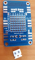
To experiment with RF and a VNA a clever designed test-board kit exists so i ordered one.
https://www.sdr-kits.net/DG8SAQ-VNWA-Testboard-kit
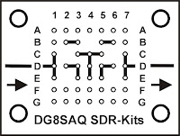
Row A, F, G, B1 and B7 are all GND (In picture 2 presented as small circles)
Pad B4 C2 C6 E2 and E6 are Isolated (floating) pads (Not drawn in picture 2)
The other connections between the pads are as drawn above.
Besides the PCB with the headers some jumpers and a 50 Ohm load is needed.
As a minimum it is recommended to make
2 pcs 2-pin short
1 pcs 3 pin short
1 pcs 3 pin jumper
1 pcs 50 ohm load
Also having a 2-pin open as reference can be useful
The 50 Ohm load can be made by using 2 100 Ohm 0603 or 0805 SMD resistors in parallel (Stacked on each other).
To make a through connection between the two SMA connectors place
2-pin shorting jumpers between D1-D2 and D6-D7 and a 3 pin jumper between D3-D5
A short or load (or open) can e.g. be made by placing appropriate components between E1 and F1
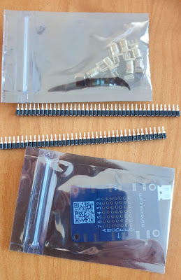
Below a picture of the kit that i did buy. It comes with the header pins and SMA connectors and 2 SMA resistors.
I did solder the headers on the PCB and also the SMA connectors.I measured some of my resistors, trying to match 2 resistors to get close to 50 Ohm. However finally i just used two random selected resistors as, when measuring with my ohm meter, my 100 Ohm resistors all seemed to be just below 100 Ohm.


No comments:
Post a Comment